
TMSC & ASML, post Q3 analysis and outlook
Plus Micron, HBM, CoWoS, and a variety of other topics

TSMC
Company profile: TSMC is the leading foundry in semiconductors with a global market share of over 50%. The foundry industry manufactures the chips for the semi designers — such as Nvidia, Qualcomm and Marvell — and they are largely based in the far east i.e. Taiwan, South-Korea and China. Although Intel is now in the process of becoming an US based foundry.
TSMC returned to revenue growth this quarter with 10% quarter on quarter growth (in USD) as the latest 3nm node started to ramp up, AI-related demand continued to be strong, while also the smartphone market returned to growth. The company guided for another 11% quarter on quarter growth in Q4, however, cautiousness on the near term outlook remained as fabless customers are still working through inventories. This is reflected in consensus numbers for both Q1 and Q2 of next year:
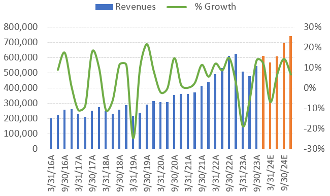
Revenues are now expected to be down mid single digits this year, with the company returning to 20% growth in ‘24 and ‘25 on the sell side’s numbers:

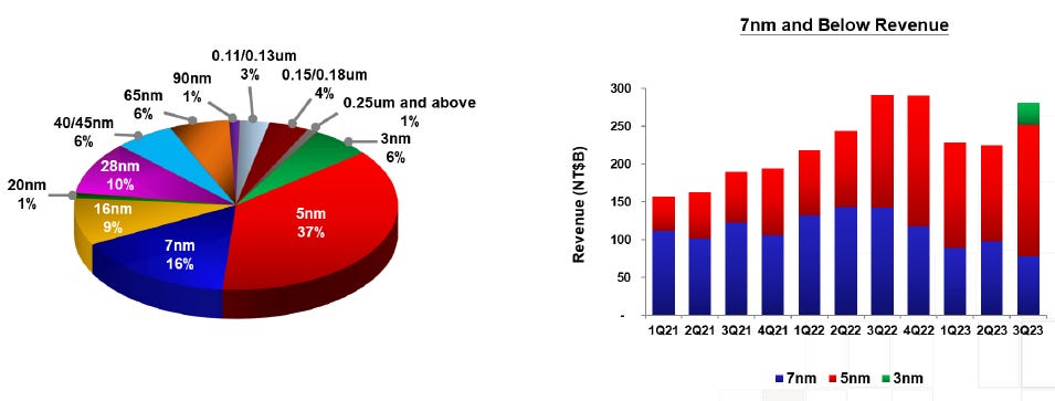
The chart on the right below shows how the 3nm node (N3) provided a nice uptick in revenues, with also N5 being very strong. The other on the left highlights how 3, 5 and 7nm are now the three key nodes for TSMC, contributing nearly 60% to revenues.
However, 7nm revenues came in weak — TSMC’s CEO on this topic: “Now talking about N7, the 7-nanometer technology, why we have such low utilization. In 10 years, smartphone demand dropped dramatically from about 1.4 billion units to 1.1 billion now. In this time frame, the N7's utilization has been impacted, followed by one major customer who delayed their product introduction. But saying that, we are confident to backfill our 7-, 6-nanometer capacity with additional specialty demand from consumer, RF, connectivity and other applications. And return to healthy levels of utilization over the next several years. This is very similar to a situation that we had with 28-nanometer, back in 2018 and 2019. It was underutilized for a period of time, and we worked hard to develop specialty technologies and now we have to expand 28-nanometer specialty capacity. That’s the same kind of a story.”
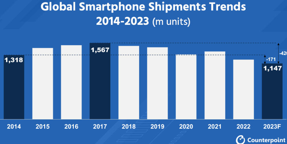
Smartphone units have been on a declining trend with consumer replacement cycles lengthening. As new versions of smartphones are not bringing in sufficiently new features, the average consumer is now keeping on to his phone for around three years.
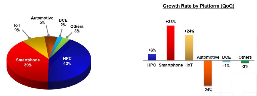
High-performance computing (HPC) and smartphones are the two key end-markets for TSMC, both contributing around 40% to revenues.
N3 will become the next large revenue driver for TSMC and is really the base 3nm process technology, offering a 15% performance improvement or 25% power reduction over N5. Subsequent technology improvements on this same node will offer even better power or performance and are called the N3E, N3P and N3X families.
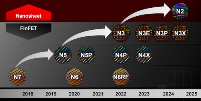
The CEO gave updated us how these are proceeding: “Now let me talk about N3 and the ramp-up progress. Our 3-nanometer technology, the most advanced semiconductor technology in both PPA (power, performance & area) and transistor technology, is already in production with good yield. We are seeing a strong ramp in the second half of this year, supported by both HPC and smartphone applications. We reaffirm N3 will contribute a mid-single-digit percentage of our total wafer revenue in 2023, and we expect a much higher percentage in 2024, supported by robust demand from multiple customers. N3E has passed qualification, achieved performance and yield targets, and will start volume production in the fourth quarter of this year. We will also continue to provide further enhancements of N3 technology, including N3P and N3X.”
He also gave a bullish outlook on their coming N2 node in 2025. This is a positive for ASML as this new node will provide the main source of order growth. TSMC’s CEO: “The recent surge in AI-related demand supports our already strong conviction that demand for energy-efficient computing will accelerate. The value of our technology platform is expanding beyond the scope of geometry alone and increasing toward great power efficiency. In addition, as technology complexity increases, the lead time and engagement with customers started much earlier. As a result, we are observing a strong level of customer interest and engagement at our N2 node, similar to or higher than N3 at a similar stage, from both HPC and smartphone applications. Our 2-nanometer technology will be the most advanced semiconductor technology in the industry, in both density and energy efficiency when it is introduced in 2025. As part of our N2 technology platform, we also developed N2 with backside power rail, which is best suited for HPC applications. We are targeting backside power rail to be in production in 2026.”
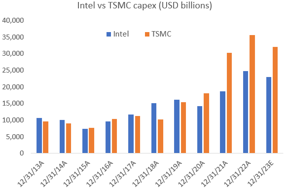
The company has vastly started outspending Intel on capex over the last three years — the battle between these two will be one of the most interesting stories in semis over the coming years.
TSMC’s commenting on their competition with Intel: “Actually, we do not underestimate any of our competitors or take them lightly. Having said that, our internal assessment shows our N3P technology demonstrated comparable PPA to 18A competitors’ technology (i.e. Intel) but with an earlier time to market, better technology, and much better cost. Our 2 nanometer technology without backside power is more advanced than both N3P and 18A, and will be the most advanced technology when it is introduced in 2025.”
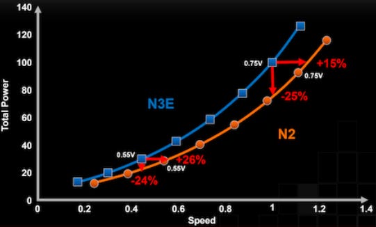
N2 will bring a power efficiency benefit of around 25% or a performance improvement of 20%. Power efficiency is increasingly growing in importance as it increases battery life in smartphones while lowering power bills for datacenters.
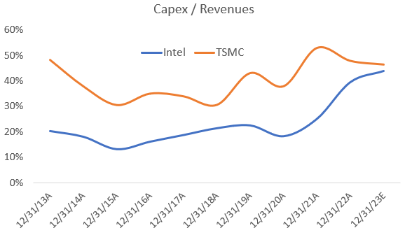
One of the biggest challenges in implementing these technology transitions are the investments required, as ever more tooling is needed at each new node. One can clearly see the industry’s rising capex intensity over the 2018 - 2023 period. Naturally this correlates with the strong performance of the semicap industry.
TSMC’s CEO commenting on this: “If you ask me, what is the most challenging part, I would say it’s cost. You look at it today, inflation and everything, the tools have become more and more expensive. Although we can do it on time to meet our customers requirements, our challenge right now, is to reduce the cost so more customers can afford it. But even with that, we have a lot of customers interested and engaged.”
While the company is guiding for their capex to keep increasing, they think they’ll be able to bring down the capex intensity (i.e. capex relative to sales) in the next few years from currently elevated levels. Long-term, TSMC reckons that they can return to mid thirties capex intensity levels. However, they also gave a rosy picture on their capex projections in 2018, whereas investors who were listening to ASML at the time were the ones who turned out to have a better feel for what was coming..
AI
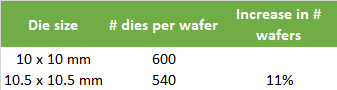
The AI end-market is currently contributing a bit more than 5% to the company’s revenues. TSMC’s CEO discussed the trends they’re seeing in this area: “AI demand continues to grow stronger and stronger. Edge devices including smartphones and PCs, are starting to incorporate AI functionality. We observed neuro engines have been added increasingly. So, the die size will increase, even if the units did not increase dramatically. The die size has mid-single digits increases so far and I expect that this trend will continue. And we expect more customers will put AI capabilities into their products. But we are still quantifying the impact from this development. So we’re maintaining the previous statement that we expect it to grow to about mid-teens of our revenue in five years. And AI will need very power-efficient chips in edge devices, especially when it is mobile. So I do expect that my customers will move into the leading edge node more quickly to compete in the market.”
Mid single digit increases in die size might not sound like much, but these increases are leveraged in terms of the number of wafers needing to be processed:
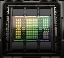
The main bottleneck for Nvidia — TSMC’s large AI customer — in meeting all of its massive, current GPU demand is on the advanced packaging side, i.e. CoWoS. This is a 2.5D packaging technology developed by TSMC to interconnect dies side-by-side on an interposer, allowing both for high-bandwidth and high-speed communication. In the case of Nvidia’s flagship H100 GPU for example, the central GPU die is connected to six stacks of high-bandwidth memory surrounding it:
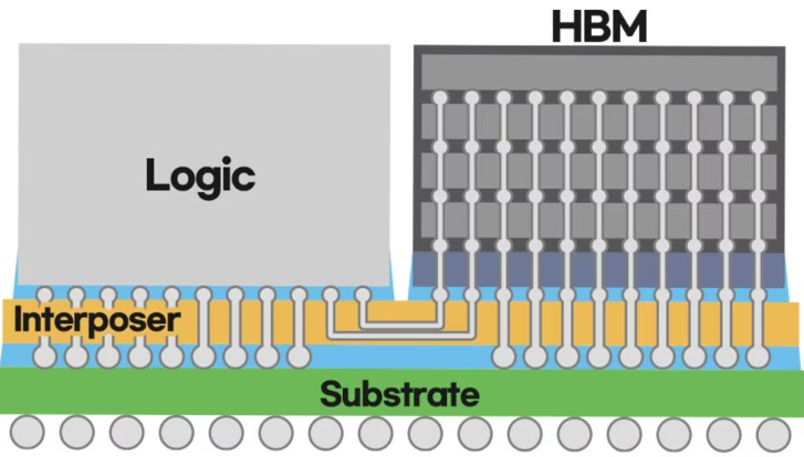
Samsung illustrates how this works schematically — a vertical stack of HBM units are interconnected to a logic die via the interposer, with the substrate providing the input-output to the board:
TSMC has sufficient 5nm capacity to meet AI demand, but clearly got caught out on where exactly this 5nm demand would come from. Currently these AI chips are the main driver of CoWoS demand. TMSC’s CEO gave us an update on the situation: “The last time we said that we will double our CoWoS capacity and we are working very hard to increase the capacity more than double, but today we are limited by our suppliers’ capacity. So we still maintain that we will double our CoWoS capacity by the end of 2024.”
Nvidia is also working with other packaging firms such as UMC and Amkor to dual-source CoWoS capacity, but I’m suspecting that TSMC will continue to get the lion’s share of advanced packaging orders.
Overseas fabs
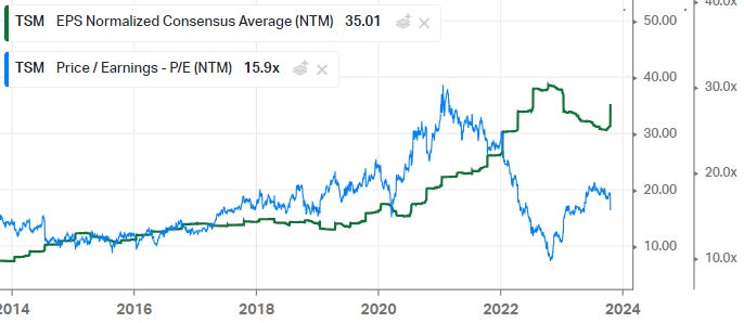
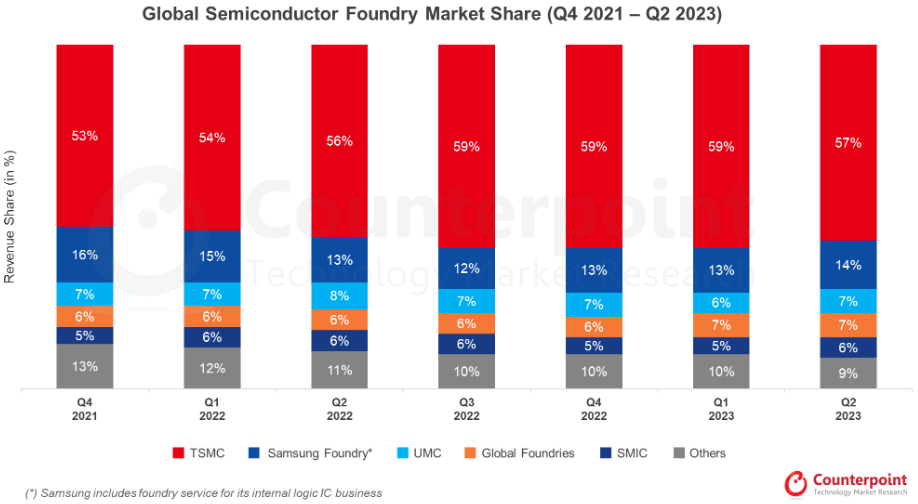
TSMC is currently only trading on 16 times next-twelve-months’ EPS, despite having been a solid EPS compounder over the last decades while enjoying a dominant 57% global market share in the foundry industry.
TSMC’s dominant market share by quarter:
I have previously speculated that for every 10% of revenues the company can relocate its manufacturing capacity outside of Taiwan, its PE multiple would rise with 1.5 points. Theoretically, if 100% of revenues would come from overseas, this would make its multiple trade on 31x, which would be more in line with its peers:
TSMC is currently building four overseas fabs. Making a number of assumptions, these could contribute around 15% to 2027 revenues:
Both Europe and Japan will be specialty fabs producing a variety of technology nodes targeted at the automotive and industrial end-markets. The European fab will be based in Germany with NXP, Bosch and Infineon each also holding a 10% share. In all three geographies, governments are sponsoring these investments with subsidies contributing around one third of invested capital.
TSMC’s CEO updated us on developments here: “We are making good progress on the infrastructure, utilities, and equipment installation issues in our first Arizona fab and the situation has improved. We have hired close to 1,100 local TSMC employees so far. Many of them have been brought to Taiwan for extensive hands-on experience in our fabs so that they can further their technical skills, being emerged in TSMC’s operating environment and culture. We continue to target volume production of our N4 process technology in the first half of 2025 and are confident that once we begin operations, we will be able to deliver the same level of manufacturing quality and reliability in Arizona as from our fabs in Taiwan.
In Japan, we built a specialty technology fab, which will utilize 12, 16, 22 and 28-nanometer technologies. We have hired approximately 800 local TSMC employees so far with the majority having brought to Taiwan for experience. Equipment moving has begun this month and volume production is on track for late 2024.
From a cost perspective, the initial costs of overseas fabs are higher than fabs in Taiwan due to smaller scale, higher costs throughout the supply chain, and the early stage of the overseas semiconductor ecosystem as compared to a matured ecosystem in Taiwan. Our responsibility is to manage and minimize this cost gap while our pricing will also reflect the value of geographic flexibility. By taking such actions, TSMC has the ability to still deliver the long-term gross margin of 53%.”
So TSMC’s pricing will be higher if clients want to opt for the more secure, local supply chains. Naturally some of this you can get back as a client due to lower transportation costs and lead times.
Financials
The US introduced fresh export restrictions for China this week, TSMC’s CEO commenting here: “We are still doing our assessment. But so far, we can tell you that the impact to TSMC is limited and manageable in the short term. For the long term, we are still evaluating what will be the consequence.”
At 10x EBITDA and 18x EPS for 2023, this is obviously not an expensive name. The expected FCF yield for next year is above 4% while the company is sitting on USD 18 billion of net cash.
The company also did seem cautious on the margin front for the coming years, TSMC’s CEO: “In the past, our leading node normally reaches corporate gross margins in about 8 quarters. But as we progress with more leading nodes, it will become more challenging as the leading node is becoming more and more complex. Also, in the past few years, the inflation pressure that was not expected also contributed to the higher cost in the N3. So it’s going to be pretty challenging for future leading nodes to reach corporate margins in the same timeframe. For the mature nodes, gross margins are really congregated around the corporate average in a pretty narrow band because we focus on specialty technology. It’s not a commodity capacity.”
Reading the above, perhaps there could be some disappointment on the margins for the market.
ASML
You can find an introduction to ASML’s business here.
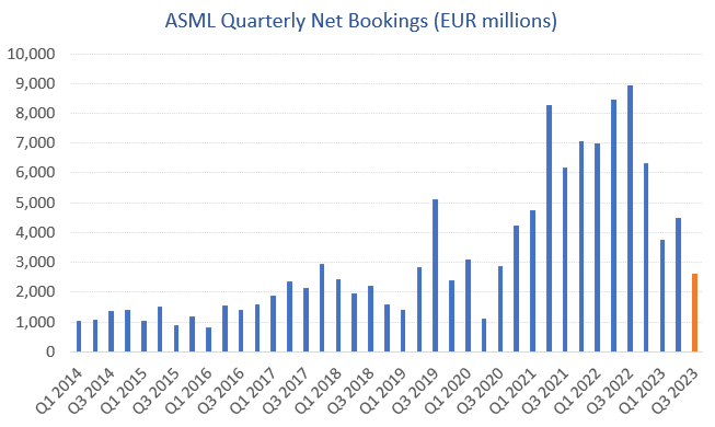
Obviously ASML’s booking numbers for Q3 were weak coming in at EUR 2.6 billion:
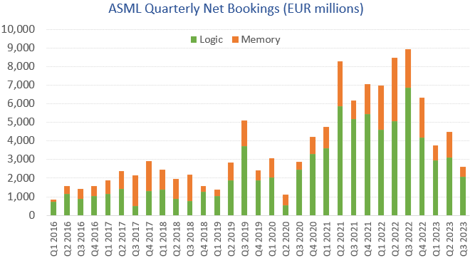
If we disentangle this data by end market, we can see that memory orders have nearly evaporated while logic is still holding up much better:
ASML’s CEO discussed the current state of the semi industry: “The industry seems to be passing through the cycle trough. There has been some improvement in end-market inventory levels downstream, although inventory levels upstream remain elevated. While lithography tool utilizations are still running at levels lower than normal, tool utilization in Logic continues to show signs of improvement while Memory has yet to turn. We expect to see an inflection point indicating the start of a recovery by the end of the year, although the shape and slope of the recovery remains uncertain. Looking further ahead to 2025, we expect significant growth since more than 50% of our EUV and DUV shipments will go to new fab projects. On top of this, we expect existing fabs will be adding capacity driven by a continued recovery cycle.”
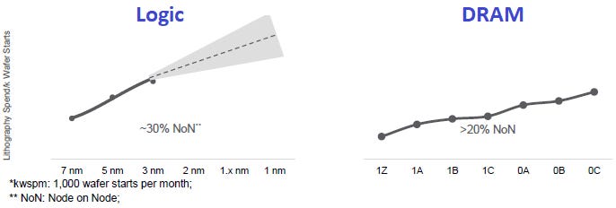
The bullish 2025 outlook comes from the company’s logic customers moving to their 2nm node in that year which will require more EUV and immersion tooling, as well as the DRAM industry requiring more EUV at the coming 1-gamma node. ASML estimated that DRAM then should start making up 30% of EUV volumes. The company has in the past presented the following slide how litho intensity moves up as logic and DRAM customers progress from node to node:
As transistor architectures keep shrinking node on node, more litho equipment is needed in the manufacturing process to handle increasing patterning needs. NAND isn’t part of this trend currently as transistors aren’t scaling anymore. Instead, the cost per bit is being reduced by stacking memory cells vertically on top of each other, a process which will move beyond 1,000 layers in the future. This process is especially more etch intensive — and so Lam Research is a clear play here — but also more deposition intensive, which we discussed last week when reviewing atomic layer deposition and ASM (not to be confused with ASML).
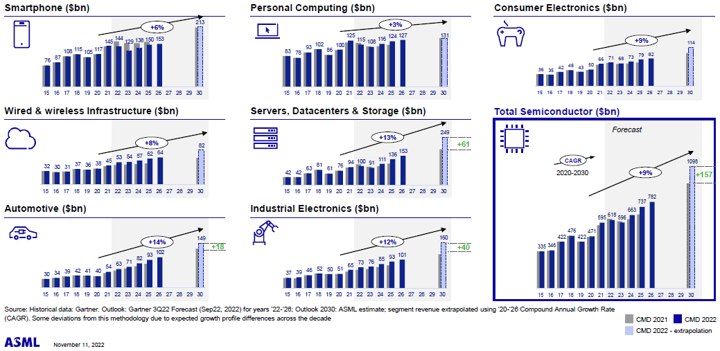
The other long term propellant for ASML should be the growth in the semiconductor market, which is expected to grow at a 9% CAGR during the current decade. The three fastest growing end-markets here are datacenters, automotive and industrials. Obviously with the boom in AI and transformer-based models in particular (e.g. ChatGPT) the growth rate is likely to move up, as these models happen to be much more compute and memory intensive, both in the datacenter as well as in edge devices.
On the last call, ASML’s CEO was still looking for revenue growth in 2024 but he downgraded this now: “We expect 2024 to be a transition year. Based on our current perspective, we take a more conservative view and expect a revenue number similar to 2023. But we also look at 2024 as an important year to prepare for significant growth that we expect for 2025.” Obviously the disappointing result this quarter will have been a factor in the downgrade.
Current sell side revenue estimates for ASML are highlighted below. Post 2024, analysts are looking again for double digit annual revenue growth. The company is currently sitting on a EUR 35 billion backlog so at the current run rate of around EUR 7 billion of revenues per quarter, the coming five quarters are already in the bag. Therefore it shouldn’t be a problem hitting that expected revenues number for next year. However, to see strong growth indeed being generated in ‘25, we will need to see a pickup in orders during the first half of ‘24.
ASML’s CEO gave some details here: “Our lead times are more than 12 months. For EUV they are 1.5 years. So we need to have that very close connection with our customers. And we have these insights into these new fab expansions, not so much where they’re going to add capacity for the existing fabs because that’s basically a question of where the cycle is. If we look at the demand that we’re currently discussing with our customers, then 2025 is a very strong year and we would have to see the order recovery in the first half of 2024.”
Memory
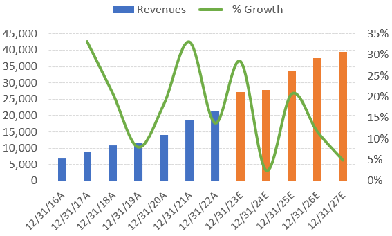
The memory industry has gone through a brutal correction over the last year. However, green shoots are emerging here as well with Micron’s August quarter seeing for the first time a clear revenue uptick. While Wall Street is seeing a sustained recovery over the coming year (orange bars).
The reason ASML’s CEO is still cautious on this end-market however is that the memory industry installed large amounts of production capacity during the covid semi boom. And so now underutilized tools are being redirected to transition to the next technology nodes, as opposed to ordering new equipment. Micron’s CEO detailing this on their recent call:
“As you know in 2023, the industry has experienced extreme oversupply and extreme negative effects on the profitability as well. And you see now that capex cuts and underutilization in the fabs have been implemented across the industry. At the same time, the demand for new products is increasing that require leading edge technology. And in order to maintain our supply discipline, and to meet the demand for these new products such as HBM, such as GDDR5, we are shifting some of our equipment from older nodes into the newer technologies to ramp those up into production. In the past, we would have done this with more capex, but we are being extremely mindful of capex spend, extremely disciplined about supply. And as we pointed out, the new products in the leading edge nodes also do require more wafer capacity for the same gigabits of production given the nature of HBM, where the die size is twice as big. So these new products actually also have a favorable impact on the industry supply growth capability.”
The DRAM industry actually has consolidated fairly well over the years which makes it easier now to install this discipline in the industry.
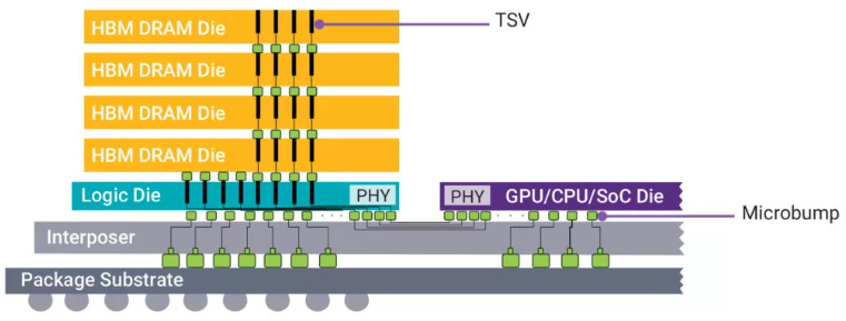
High-bandwidth memory (HBM) is the type of DRAM which is integrated next to the GPU die(s) with 2.5 packaging for AI applications. It allows for large amounts of working memory to be available at very close proximity to the accelerators. Synopsys shows how it also could be placed on top of a logic die with 3D packaging (below). However, the main application currently remains 2.5D packaging in AI accelerators.
NAND is still more competitive with also Chinese player YMTC entering. Whereas DRAM is mostly a three player market, NAND would become a six player market if YMTC takes a decent share. However, YMTC is currently looking for local Chinese suppliers to replace parts in their Lam tools, where also the servicing flow has been halted due to US export restrictions.
The key question for ASML is — when will the memory orders return? Micron’s CEO gave us a hint: “There will be new capex investments required, which of course will require increased pricing, increased margins, and improved cash flow for us to justify that capex investment to increase wafer capacity again.”
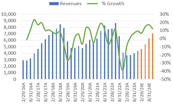
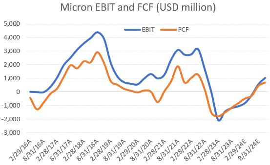
So obviously restoring both the demand-supply balance and industry profitability is a key priority for Micron and I suppose competitors as well. However, as AI is both DRAM and HBM intensive, I also suppose that the temptation will be large to start investing at some stage. Micron’s recent presentation mentions that “We see our demand at leading-edge nodes exceeding our supply in fiscal and calendar year 2024, particularly in the second half of the year.” I’m reading this that healthy profitability should return in the second half of next year. This is also when Wall Street is modelling Micron’s EBIT and FCF to turn positive again (chart below). So this should be translating into order flow for ASML I suspect at the latest around the second half of next year. There’s a good chance we could see orders earlier due to ASML’s currently long lead times.
HBM is obviously the most interesting market due to its high exposure to AI and high capital intensity. Micron was late to the party here with pioneer SK Hynix taking a 50% market share. However, the company seems to be catching up with Micron’s CEO commenting: “We have skipped the HBM3 generation. We commercialized HBM2E and we went straight to HBM3E in order to get ahead. And we are very excited about this technology because the samples that our customers have in their hands have industry-leading performance. The production ramp-up which will start in early calendar 2024, will be pretty big in the back half of ‘24, and then build from there into ‘25. And our goal is to ensure that we get our HBM share to be similar to our DRAM supply share and to get there as soon as the ramp will allow.”
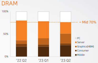
The HBM market is also becoming sizeable due to the boom in AI — HBM contributed 20% to SK Hynix’s DRAM sales last quarter:
Obviously HBM could be interesting for ASML, and if the boom in AI is sustained this could bring in meaningful orders next year.
China
China is currently a big driver for ASML’s shipments, contributing over 20% of sales this year with a similar amount left in the backlog. The main driver here are the mid-critical to mature Chinese fabs addressing the automotive, industrial, IoT and green tech end-markets. These Chinese fabs have been receiving less than 50% of their demand over the last two years so there will still be some catch-up to do.
The company’s CEO also discussed the recently added export controls by the Biden administration: “On the geopolitical front as it relates to export controls, the US government yesterday published updated export control regulations. Given the length of the document, we need to review the final regulation thoroughly and make a detailed analysis, which will take some time. The export control measures could have an impact on the regional split of our shipments in the medium to long term, but we do not expect an impact on the global demand scenarios as communicated during our investor day in November last year, since the long-term growth perspectives for our industry remains clearly unchanged.”
I agree on this take on the long term demand as at this stage it seems unlikely that China will be able to build up a competitor in immersion DUV technology within five years. Both immersion and EUV are currently the bread-and-butter tools for ASML, and so if all these tools would be banned from being sold into China, which is very possible at this stage, this would mean that if the Chinese don’t have a homemade immersion tool, they simply would have to buy the manufactured semis from elsewhere. Meaning that these fabs will have to be built outside of China by non-Chinese firms.
China’s lithography player SMEE currently has a 90nm tool, which is really stone age technology these days, and is looking to launch a 28nm tool this year. However the question is really what the productivity of this tool will turn out to be. ASML is vertically integrated on some of the key components while having been making continuous productivity improvements to their tools over the years, both on the hardware and software side (algorithms). Therefore I suspect it will take a considerable amount of time before SMEE’s tool comes anywhere close to ASML’s productivity at 28nm.
Currently ASML’s low end immersion tool, the 1980, is still allowed to ship into China if it is used in lower end fabs. However, how can the US enforce that these tools won’t be sold to higher end fabs in the second hand market afterwards? Practically all of ASML’s manufactured tools over the past decades are still running, so their mileage is massive. It looks that once again these rules have quite some holes in them.
ASML’s CEO detailed this: “So the way we read the rules now, the principle is that the 1980s would fall under the export control restrictions, but only when those immersion tools are used for advanced semiconductor manufacturing. And we’ve been informed that only applies to a handful of fabs. So that means that the 1980 for those handful of fabs is off limits, but not for the vast majority of our Chinese customers for which we don’t need an export control license either. We can just ship. And those are for the mature and lower mid-critical chips that are needed for all the transitions that I just mentioned. So on the question what percentage of the shipments that is now excluded, it’s anywhere between 10% and 15% (of Chinese shipments). So the vast majority is mature and mid-critical and that is what basically will remain.”
Financials
The sell side’s estimates below — ASML is trading on 28x this year’s EPS, a nearly 3% 2024 FCF yield, and with a healthy EUR 3 billion cash position.
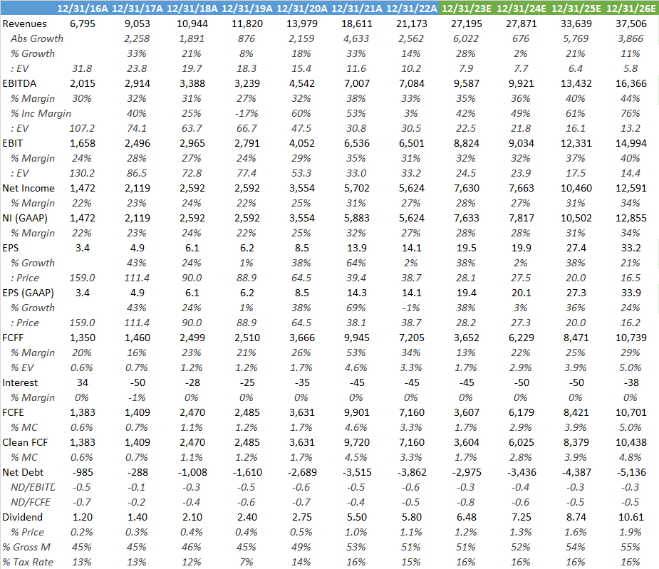
At their latest capital markets day, ASML updated their long term model for 2030 — investors who paid attention to their previous long term 2020 model made handsome money as it turned out to be spot on. In 2030, even if the company would hit the low end of their guidance and the shares de-rate to a 25x PE, one could still make a double digit annualized return (IRR). I’m also factoring in ASML continuing to buy back shares at a rate of 2.3% per annum, which reduces the share count by 2030 and lifts EPS.
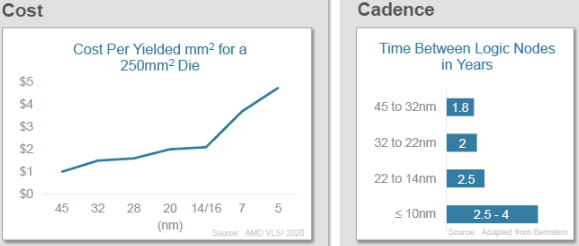
The main risk for ASML is the semiconductor innovation roadmap continuing to slow down, which would result in order flow per node getting spread out over more years, lowering annual revenues. The other risk is on the economics, with the cost per die area having taken on a much steeper slope post 16nm. However, additional costs can be partly recuperated from lower energy bills due to the efficiency gains of smaller transistor sizes. Additionally, these next-gen transistors bring other benefits, such as faster computations, more calculation power, and longer battery lifes. I suspect most of the leading edge customers, e.g. Nvidia, Apple and AMD, will continue to be happy to pay for this, also as they need to differentiate their products anyways.
If you enjoy research like this, hit the like button and subscribe. Also, please share a link to this post on social media or with colleagues with a positive comment, it will help the publication to grow. All shares are appreciated.
I’m also regularly discussing tech and investments on my Twitter.
Disclaimer - This article is not a recommendation to buy or sell the mentioned securities, it is purely for informational purposes. While I’ve aimed to use accurate and reliable information in writing this, it can not be guaranteed that all information used is of this nature. The views expressed in this article may change over time without giving notice. The future performance of the mentioned securities remains uncertain, with both upside as well as downside scenarios possible. Before investing, I recommend speaking to a financial advisor who can take into account your personal risk profile.
Great analysis and update. Thanks
Excellent writing and charts🔥🔥