

Introduction - the Chip Design Flow
We’ve written extensively on EDA (electronic design automation) software in the past. For newcomers on the topic, a recent expert call with a VP at Analog Devices gave a good overview of the space:
“EDA varies if you’re doing digital or analog design. Let me start with digital because that’s where a lot of companies are focused. In doing digital design, you start with a specification of what you want to build. That specification is normally in some form of natural language. That specification is then converted into the front-end logic design, where engineers use the different logic components to implement that design. After this design phase is the RTL generation phase.
RTL is actually the code to implement the design—this can be in something like Verilog (a hardware description language used to model electronic systems). That RTL then goes through a verification step. Essentially, we test that logic to make sure it’s working properly. After that phase is complete, the back-end or physical design phase happens, where you physically map the logic design to the chip area that you want to implement. Once the physical design is complete, another round of testing is done to make sure all the logic, all the timing is all still working.
Only after that final phase of testing the physical design is the design ready for tape-out in manufacturing. Those are the high-level steps to build a microcontroller or some form of digital design. Most semiconductor companies will leverage a lot of software tools to help them through these different phases. The two most common partners to work with on this whole workflow are companies like Cadence and Synopsys, and Siemens as a third. They make this much easier by providing an integrated workflow to accomplish these different phases.
We use both companies. Cadence we leverage for a lot of our analog design and Synopsys for a lot of digital design. We’re leveraging their flows pretty much end-to-end—all the way from the front-end tooling for RTL creation, their compilers, their DV (Design Verification) test benches, all of it. These companies provide tools like simulators as well, so that once you start building your design, they provide a lot of capability to simulate that. That’s part of the testing phase.
I’d say that the most painful step, or the one that probably takes the longest and is the riskiest, is design verification (DV). It’s essentially testing the design and like most technology—whether it’s software or hardware—getting all the corner cases, generating what are called behavioral assertions, this is probably the hardest part of any design. We struggle with this constantly to get the proper test coverage. The RTL development simulation is not that complicated compared to the DV test bench at the end. There’s also going to be some challenges on the physical design, the place and route, and all the timing closure, getting it physically to fit within your constraints.
We also leverage different types of IP from these companies, so we license parts of the design. Those individual IPs have existing test benches, that already exists. What becomes more bespoke is when you take their IP and combine them with a bunch of our internally developed IPs, and then you integrate all that into a SoC. The corner cases at the SoC-level are new and you have to create new test cases for each individual device. Think of it as the components are individually tested, but when you integrate them it becomes a challenge.”
Although Cadence was historically stronger in analog, they’ve been closing the gap in digital semi design with Synopsys. This was another good recent expert call with a semiconductor veteran who’s now on the board of Baya Systems (a startup in Silicon Valley working on chiplet connectivity):
“I did start-ups, four of them. Two of them ended up ultimately becoming a part of Synopsys, and then one of them IPOd. You can’t think of Cadence without thinking about Synopsys because it’s a duopoly. If you are designing chips, you are going to use both companies. They have similar histories of how they were started. Some of the same people went back and forth between the companies. Think of them as utilities or tools that, as semiconductor design was starting to use PCs and mini computers, these little tool companies started merging to become what is now Cadence and Synopsys. Combined, they have 80%+ of the market in most sub-segments of EDA. Even semiconductor IP, they’re very big there.
As far as the business model, both of these companies, when you’re dealing with the larger companies, they have a license that might be three years or five years. For smaller companies, it might be something that’s more token based, you generally don’t get all-you-can-eat for all your engineering employees to use the tools. You get a more restrictive license—and probably a higher margin license for the EDA companies—than what the big companies have.
The EDA companies work together with the fabs to create PDKs, process development kits. When TSMC, or Samsung, or Intel, come out with a new process, they work with the EDA vendors to create the kits that the end customers will use to make their designs that target a particular semiconductor process. There’s a ton of engineering work that goes into creating these PDKs. Intel has always sucked at this. Intel has gotten better, but the first time they tried to become a fab, it was impossible for anybody to use Intel’s process, except Intel, because they didn’t have a PDK.”
The EDA Crash
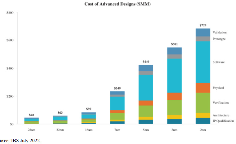
The EDA space has been a very attractive space for investors over the last decades. A duopoly meant strong pricing and high margins, while the recurring nature of software revenues meant that these companies weren’t exposed to the brutal cyclical swings of the semiconductor industry. At the same time, as the cost of advanced semi design exploded in the EUV era, both Cadence and Synopsys enjoyed a massive tailwind to grow their revenues with advanced semi design costs surging node-on-node:
The above tailwinds will remain valid in the foreseeable future. However, Cadence and Synopsys shares are down around 14% since Moonshot’s Kimi K3 autonomously designed a functional semiconductor chip in 48 hours, using exclusively open-source tools. The chip was a 4mm² die running at 100MHz on the freely available Nangate 45nm Open Cell Library—designed, verified, and simulated entirely without human intervention.
A few points to note here. First, the Nangate 45nm Open Cell Library isn’t a PDK and has no foundry behind it. Nangate was absorbed into Silvaco years ago—a small and low-end player in EDA—and the library is basically the “hello world” of open EDA research (constructing a “hello world” program is the typical introduction for students to any new programming language).
The problem with open-source EDA tools, however, is that these tools don’t have access to any advanced PDKs. The EDA duopoly has a large moat—not only is decades of semi design know-how ingrained into these tools, but these tools are also the only ones with access to advanced PDKs. For example, TSMC certifies tools through its Open Innovation Platform, and that list of tools is: Cadence, Synopsys, and Siemens. Then, these PDKs are also only available to TSMC’s approved customers and under strict licensing agreements. Obviously, foundries don’t give away their state-of-the-art IP.
So, what open-source EDA tools actually have access to is a much older tier of the stack—TSMC 65nm, GlobalFoundries 12nm, and Intel 16nm processes. Even if you want to design a TSMC 65nm chip, you still need a TSMC license, so it’s not open to everyone. The only fully open PDKs are very old processes, such as SkyWater 90nm and 130nm, and GlobalFoundries 180nm.
Most of the money in semis is made on the advanced nodes, and there really is no other way than using the established EDA tools if you want to design chips on those nodes. For example, TSMC requires a Synopsys PrimeTime static timing analysis before tape-out. Looking at TSMC’s revenue split, older nodes—where open source tools are competing—are a very small part of the business:
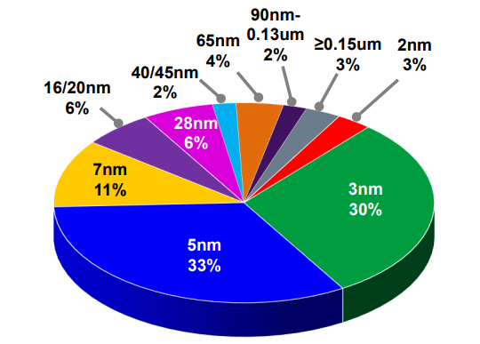
Given the semi industry’s large skew—both in terms of revenues and R&D—towards advanced nodes, we suspect that a high proportion of Cadence and Synopsys revenues are coming from the advanced nodes.
The Massive AI Opportunity
We’ve written extensively on the opportunity for EDA vendors to play a larger role in the semi design flow in the future with AI automation. Goldman recently published an in-depth report with a similar conclusion, and calculates that this represents a large opportunity for the EDA names that the market is missing:
“Consensus has viewed Cadence and Synopsys as “defensive” 12%-15% growers at best, and potential victims of AI disruption at worst. However, our new analysis suggests the shift toward custom AI silicon has exacerbated a structural shortage of chip design engineers that EDA companies are uniquely positioned to monetize with Agentic AI—an incremental opportunity we estimate at ~$3.7bn/year by 2030, which is not reflected in Street estimates and may start to be evident as early as 2H26. We believe consensus reflects the “pre-AI” version of the industry as growth is about to inflect, creating an opportunity in the stocks today.
Chip demand could drive a global shortage of ~72,000 chip designers by 2030. A key industry benchmark study (SIA/BCG, 2022) projected a ~23k shortfall in US chip designers before generative AI. Since then, hyperscalers and AI labs have launched custom silicon programs requiring at least ~2,500 designers. Meanwhile, the supply of human designers grows at just 2%-3% annually. We estimate AI design tools can add ~48k agentic engineer-equivalents by 2030, which can partially close this gap.
We size the Agentic AI revenue opportunity for EDA at ~$3.7bn annually by 2030 based on modest adoption assumptions. We estimate “Copilot-style” AI EDA tools could price at ~$25k per engineer annually, relative to the ~$90–$100k customers spend in EDA per seat. We also think autonomous agents, which both EDA vendors will launch in 2026-27, could handle up to 30% of work by 2030 at ~$50k per agent—or ~25% of the fully-loaded cost of a human design engineer.
Street numbers reflect essentially none—and we believe initial proof points could be evident within months. Consensus models both companies decelerating revenue growth from here, implying zero credit for this new Agentic layer. We estimate that this opportunity could lift Cadence’s revenue growth from ~13% to the mid-20% range (+$2.30 of EPS by 2030) and Synopsys to ~20% (+$2.20). 2H results could provide the first evidence of this growth opportunity. If agentic AI tool adoption gains traction, we believe CDNS/SNPS could re-rate in terms of faster growth rates and higher multiples.”
Is Goldman correct that AI will represent a massive opportunity for Cadence and Synopsys? Or are they missing something? Fortunately, we have a lot more insights that we came across, we’re not even halfway yet through the analysis. We’ll go through these findings next.