

Introduction to MEMS & OCS
MEMS used to be a fairly dull corner of the semiconductor industry and so historically, we’ve paid very little attention to this market. However, this is changing as optical MEMS are the backbone of one of the most cutting edge markets in the AI data center with optical circuit switching (OCS). In addition, MEMS will see long term growth from physical and edge AI in end-markets such as robotics, drones, satellites, IOT, etc.
In the AI data center, servers typically rely on layers of electronic ethernet switches to communicate with each other. The problem is that converting signals each time from the optical domain to the electrical one, and then back into optics—i.e. optical-electrical-optical conversion—takes a lot of power, and so it makes sense to keep that signal fully in optics in the first place. This is where OCS comes in.
At the heart of OCS are MEMS-based optical switches, which are basically movable micromirrors. These have a very simple function—redirect an incoming optical signal from one channel into another to reroute traffic. Yole illustrates what this looks like:
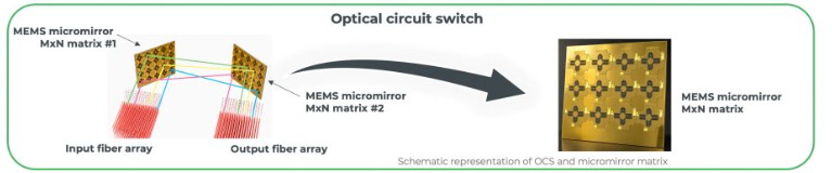
Each input-side mirror can be oriented toward a corresponding output-side mirror, effectively creating an MxN optical switching cell. The win is that OCS cuts power consumption by up to 40% to 50% compared to equivalent electrical switches. It also introduces near-zero latency because light moves through the switch at the speed of light in glass/air.
There’s one big drawback however—switching speed. MEMS mirrors are mechanical devices. Moving a physical mirror takes time—typically between 1 and 10 milliseconds, compared to traditional electronic switches that can route data in nanoseconds. Because of this millisecond-scale switching speed, OCS cannot be used for dynamic, packet-by-packet routing. Instead, it is used for a particular topology reconfiguration, for example, for re-wiring the data center fabric to connect huge pools of XPUs for a training run that will last hours or days.
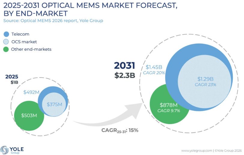
Yole expects the optical MEMS market to grow at a 23% CAGR—OCS is the market in the light blue bubbles:
Silex Microsystems & MEMS Manufacturing
Silex Microsystems is the largest MEMS foundry in the world and was recently IPO’d in Stockholm. The company manufactures the optical MEMS for Google’s OCS. From the founder:
“I founded the Company together with four other PhD students from KTH Royal Institute of Technology in Sweden, with the aim of creating a pure-play MEMS foundry fully dedicated to manufacturing MEMS based on customers’ designs. The Company swiftly outgrew its research laboratory origins, shifted to a new production facility in Järfälla, Sweden, and in 2009, transformed the MEMS industry by introducing the world’s first 200-millimetre (8 inch) wafer MEMS manufacturing fab. We have worked hard to drive the technological forefront of MEMS manufacturing since then. Today, Silex is the leading pure-play MEMS foundry globally. We have built a large customer base and long-term partnerships with many of the world’s leading technology companies.”
MEMS stands for Micro-Electro-Mechanical Systems. In simple terms, MEMS are microscopic machines which combine tiny mechanical elements such as sensors, actuators, and electronics on a silicon chip. MEMS devices usually range in size from a few micrometers to millimeters. To put that in perspective—a human hair is about 75 micrometers wide. Many MEMS components—like tiny gears, mirrors, or beams—are often just 1 to 100 micrometers in size.
MEMS are used in loads of end applications. For example, in a smartphone, MEMS detect when you rotate your phone from portrait to landscape, and they can track the number of steps you take. The same happens in Nintendo Switch controllers—MEMS motion sensors track the user’s movements to then translate them into the game.
Before MEMS, these types of devices were bulky pieces of hardware made of springs, weights and wires. However, as MEMS use the same manufacturing process as in semiconductors—i.e. photolithography, etch, deposition etc.—this allows MEMS to be mass-produced onto silicon wafers for cents on the dollar.
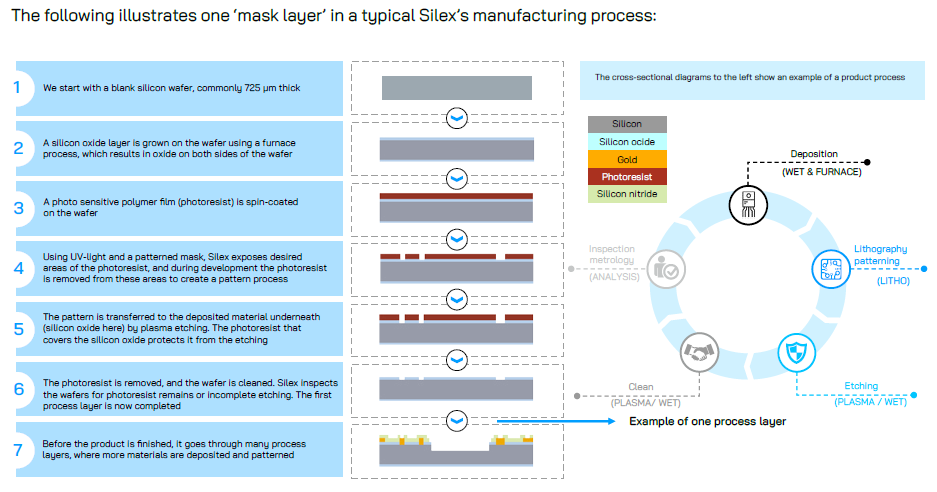
The MEMS universe is categorized by what the tiny mechanical parts actually do:
Optical MEMS: These use micro-mirrors, lenses, or gratings to manipulate light. Optical MEMS route optical signals through fiber-optic networks and drive the spinning mirrors inside lidar sensors for self-driving cars.
RF-MEMS handle high-frequency wireless signals such as in 5G infrastructure, smartphones, and radar systems.
Inertial & Acoustic MEMS measure physical motion, forces or sound waves. These track movement, rotation and sound in consumer electronics.
Microfluidic & Bio-MEMS feature microscopic channels, pumps and valves to move tiny droplets of liquid with absolute precision. These are used in DNA sequencing, “lab-on-a-chip” medical diagnostics and precise drug delivery systems such as insulin pumps.
Power & Actuator MEMS are designed to physically move or harvest energy at the micro-scale. Silex utilizes a specialized material called PZT (Lead Zirconate Titanate) in its manufacturing. This is a piezoelectric material—meaning when you apply electricity to it, it physically bends.
Silex is focused on the manufacturing of more differentiated and higher value MEMS. They deliberately avoid commoditized, mass-scale products. The attraction of this business is that once you’re manufacturing a high value component for a customer such as Google, that customer will rarely switch as the intensive R&D to set up the manufacturing process would have to be repeated at the new foundry. However, huge customers such as Google do split their orders, e.g. 75% to Silex and 25% to a secondary foundry. Dual sourcing is common practice across the semi supply chain, with few exceptions.
According to a Japanese source, Silex also pioneered Through-Silicon Vias (TSVs) in MEMS manufacturing (Sil-Via™ and Met-Cap™). Normally, connecting a tiny mechanical sensor to a computer chip requires running delicate wires out the sides. Silex brought TSVs—which are common in semi manufacturing—to MEMS. These TSVs allow Silex to stack a MEMS sensor directly on top of a chip, making the final hardware incredibly compact, hermetically sealed, and perfectly suited for high-vacuum applications like aerospace or advanced medical tech.
The prospectus explains the deep relationship between foundries and customers to bring to market a new product:
“Pure‑play foundries serve as critical enablers for Fabless companies and design‑centric customers. Their involvement often begins at the early development stage, where repeated iteration and refinement are required to reach scale production of the final MEMS. Successful scaling from prototype to production involves coordinated work across design, modelling, process engineering, metrology, and packaging.
As fabrication techniques advance, Silex believes that, in the future, MEMS can become even smaller, more powerful, and capable of performing increasingly advanced tasks, which can drive technology innovations further, making MEMS foundational for the future of smart, connected devices. The pace of technological advancements remains high, and foundries that can adapt their processes to meet the needs of diverse applications gain a substantial competitive advantage as compared to those that are unable to do so.”
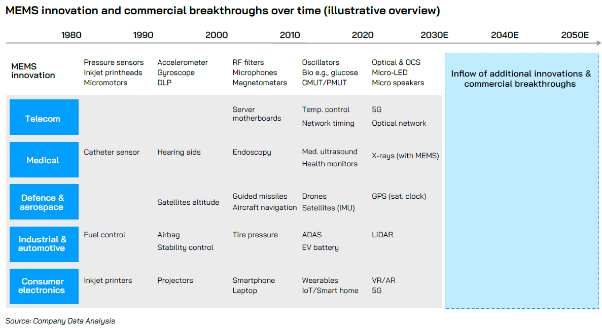
So, we also have sort of a Moore’s Law for MEMS, where these devices continue to shrink in size to enable more advanced applications. Overall, this looks to be an industry with high innovation potential and a long term growth trajectory. Silex illustrates innovation in this industry over the last decades:
MEMS are used in loads of end applications—including in high growth markets where edge AI will become important such as robotics, drones, satellites, robotaxis, IOT, etc. From the prospectus:
“Future AR display technologies are currently being served by Silex, who as a MEMS foundry is well equipped to serve the demands required to create very small form factor and complex manufacture of chips that interact with the physical domain. Silex believes it is well positioned to serve emerging device applications beyond the current defined MEMS device market, including AR display technologies that are not presently classified as MEMS devices.
The increasing adoption of MEMS across a broad range of applications has resulted in diversified demand for advanced devices. Underlying markets with rapid growth such as MedTech, AI, autonomous systems, AR and satellite communications, drive both innovation and volume in the MEMS market as new applications require novel solutions. The specialised requirements and innovative nature of these applications are expected to primarily strengthen the growth of Silex’s Focus Market.”
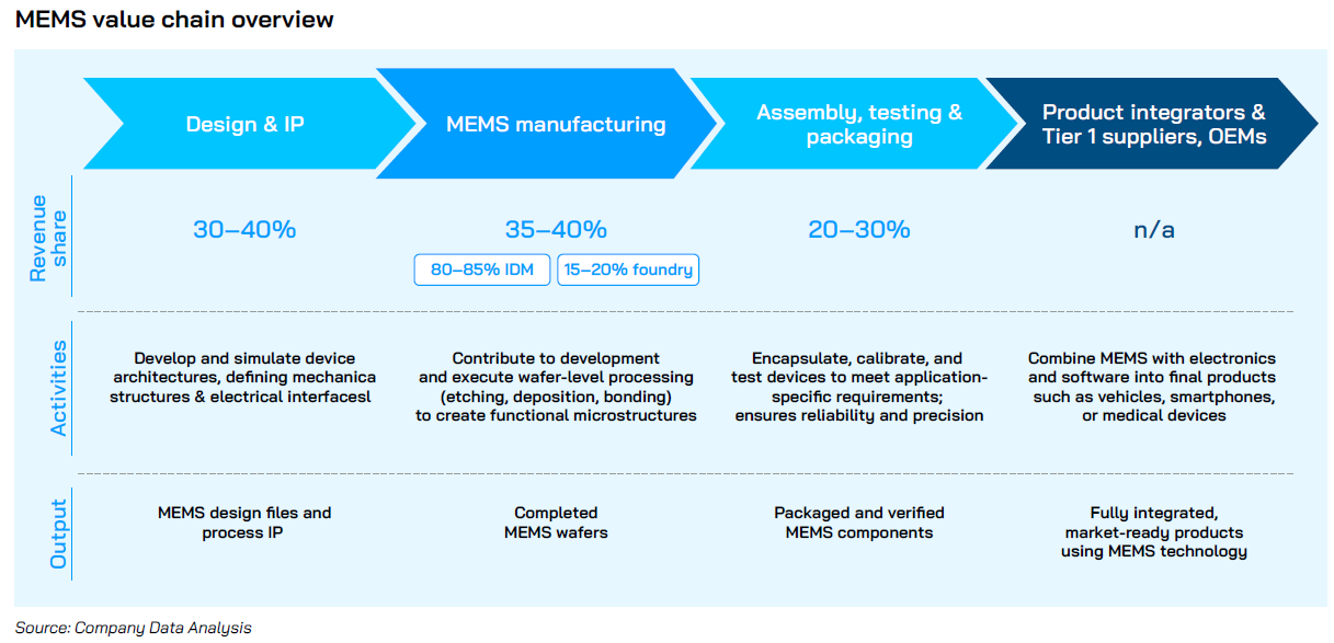
MEMS manufacturing is still largely an IDM (integrated device manufacturer, i.e. product design and manufacturing within a single company) market:
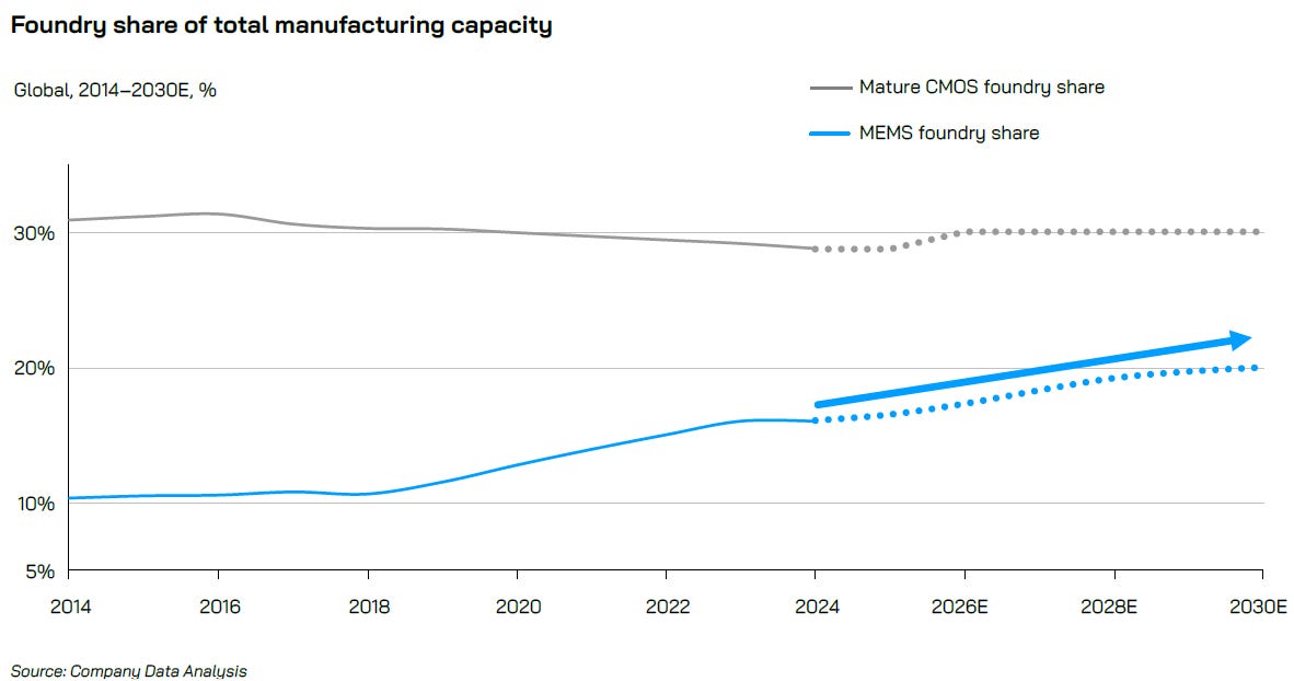
However, foundries are gradually taking share in this market, and this trend is likely to continue in the coming decades as new technologies will need specialized MEMS design and manufacturing:
Next, we’ll detail further insights into Silex Micro and the MEMS industry, with our thoughts on investing in this space. We’re currently halfway through the analysis.