
BESI & The Future of Semis
A Deep Dive

Beyond Moore’s law
While the number of transistors on a single microchip has kept doubling roughly every two years — indicating that some form of Moore’s law is still alive — the semi industry has played a trick here..
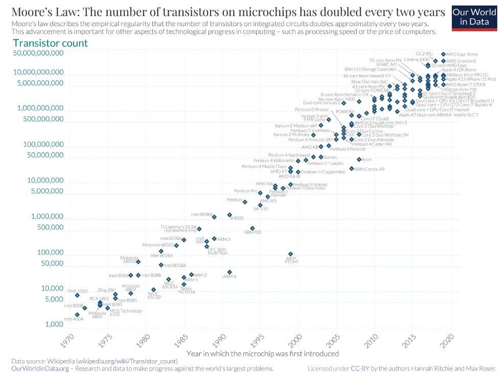
.. Which is simply to increase the die size:

A better measure of Moore’s law is whether the number of transistors within a given chip area is still doubling every two years, and here the curve started already to show a clear logarithmic pattern during the previous decade:

Under the classic definition of Moore’s law, the above trendline should have looked linear. Another problem is that the chip’s clocking speed hit a wall in the mid-2000s (the green line on the chart below). The clocking speed basically sets the rhythm at which the microchip performs calculations, similar to the drummer on an old trireme who’s setting the pace for the rowers. The faster the chip’s clocking speed, the more computations the chip can make. However, as further increases in the clocking speed gave excessive heat problems, this source of chip improvements had to be halted.

Besides increasing the size of a microchip’s die, the industry responded by simply packaging more dies within a single module to offer customers more performance. For example, AMD’s Genoa contains 96 cores across 12 chiplets (dies). Also the term chiplet is used when multiple dies are packaged together to form a single processing system.
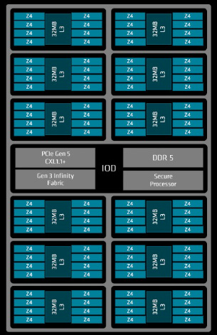
AMD’s flagship MI300 GPU goes one step further by also integrating dies vertically. In this case, CPU and GPU chiplets are stacked on top of input-output dies (IODs):

The other advantage of breaking up a computing system up into chiplets is that the compute dies can be manufactured on the most advanced process nodes of TSMC, while the less crucial chiplets such as IO can be taken care of by less expensive nodes, saving costs. This is a former VP at BESI, who was made available via the Tegus platform, explaining why chiplets are becoming more compelling:
“The game changer is that with hybrid bonding technology, you can now make a chip out of components which has more or less the same performance as a monolithic chip. There are billions of transistors on a monolithic chip, so that making a design is now very expensive. For the high-end chips, you need at least $0.5 billion in R&D costs. If you have chiplets, then you can leave everything the same and work for instance on a cache, or a core, or something else. This brings down development costs tremendously.”
And equipment accuracy becomes even more important in the assembly of multi-die systems. This is the former VP at BESI again explaining this:
“Let's consider an AMD chip, which maybe has a base chip and four cache chiplets on top, just as an example. If you start and place the first one, then the second and the third and all are good, and then you place the fourth and if the whole 3D integration is bad, all five chips go to the trash can.”
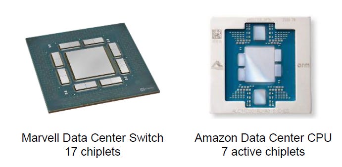
AMD is not the only one following the multi-die approach, Amazon’s Graviton 4 has 7 chiplets and Marvell’s latest data center switch contains 17:
And according to JP Morgan, also Broadcom is now developing 3D-IC based ASIC accelerators for two new customers, with one of them being OpenAI.
Whereas ASML’s tools are the key enabler of Moore’s law, as increasing patterning resolutions allow for more transistors to be built within a given chip area, i.e. to increase transistor density, BESI’s tools are the key enabler of going beyond Moore’s law, as they allow for more dies to be bonded together into a single computing system, and with more precise connections giving customers increasing bandwidths, energy savings, and space savings.
To pursue Moore’s law, the foundries at each new node have to buy both more ASML equipment and more advanced equipment to build smaller transistors. These dynamics are the key driver behind ASML’s revenue growth, resulting in ASML being a high beta play on increasing transistor densities, i.e. the semi industry’s attempt to pursue Moore’s law.
For premium subscribers, we’ll review:
How the dynamics for BESI’s future tool demand should be even more attractive than those for ASML’s tools.
BESI’s strong market positioning, especially in advanced die attach.
Industry insiders discussing the competitive dynamics in the industry, as well as BESI’s competitive advantage which explains the company’s best-in-class margins.
The various advanced packaging processes where BESI’s tools are used, and TSMC’s packaging roadmap.
How BESI benefits from the growth of networking in the datacenter.
The company’s future key role in the High-Bandwidth Memory (HBM) market.
A 2030 financial model for the company, with expected IRRs investors can make.
BESI’s current outlook and strategy, and a detailed analysis of the company’s financials and valuation, with thoughts on whether it makes sense to invest here.