

Positive sell side reports have been a major catalyst for ASML over the last month. Coverage of ASML had become widely negative throughout ‘25. There are basically two bear theses which are related. The first is that litho intensity has peaked in terms of capex requirements to move to the next nodes. The second thesis is that high-NA won’t be adopted for a while as it is not economic.
While TSMC didn’t introduce scaling at the N2 node as they moved to the new GAA transistor architecture (nanosheets in the image below), we should see scaling again at the next two nodes. This is a positive for ASML as transistor scaling requires more litho processing steps – which either need to be carried out with multiple patterning or with more advanced litho equipment (high-NA). In multiple patterning, as the name suggests, the patterning steps are carried out multiple times to transfer the needed chip patterns onto the wafer. This requires multiple processing steps with ASML’s litho tools, currently EUV or immersion DUV. The below chart is from the leading research house on transistor technology, IMEC, which basically all the key players in advanced semi manufacturing are collaborating with including ASML and TSMC:
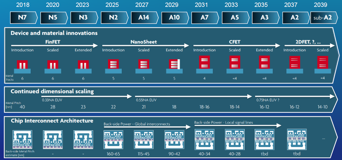
Note the metal pitch scaling on the chart above as the key driver for litho intensity. TSMC tends to pause when they move to a new transistor architecture, such as Nanosheet (GAA) this year or CFET in the future (2031E). The reason is that they want to make gradual steps to refine their processes and not implement too many changes at the same time, which can make it hard to optimize yields.
On the second bear thesis, the positive is that high-NA is much more economic than EUV at its early introduction. EUV’s uptime and productivity were extremely low. The technology had all sorts of problems and there were continuously bear theses flying around in the years leading up that the technology will never make it. The positive for ASML though is that even if high-NA gets delayed, more multiple patterning with EUV tools will be required at the most advanced processing steps. This actually increases both revenues and margins for ASML, as high-NA is lower margin than EUV due to current low manufacturing capacity levels.
This is what we concluded back in July as ASML’s shares sold off following results and weak order numbers:
“So, the long term bull case for ASML is that: 1) TSMC at its next one or two nodes will start scaling again, leading to increased EUV demand as more EUV steps will be needed again. 2) TSMC is building out three fab clusters—one in the US and two in Taiwan, where capacity requirements are increasing due to the boom in AI demand. 3) DRAM is becoming more EUV intensive, due to the scaling roadmap. AI is very DRAM intensive (HBM), boosting needed fab capacity. 4) ASML has zero competition. Thus, for long term investors, we think that the risk-reward is starting to look attractive here for ASML. The valuation is basically the same as where it was ten years ago, while a lot of tech and quality stocks in the S&P 500 have strongly re-rated (i.e. trading currently on much higher PE ratios).”
The recent environment reminded us a lot of the 2015-2016 years for ASML with bear arguments flying around such as “EUV isn’t going to work”, “Everyone already owns this stock – how can you still make money?” and “Tech is in a bubble, sell the space!”. Sounds familiar?
JP Morgan was the latest to come out with a bullish note recently:
“TSMC has started to ramp up its 2nm process and this process ramp will continue in ’26 when their lead customer, Apple, is likely to start using this process. There have also been press reports yesterday that Nvidia is expected to be the first to adopt the upcoming A16 process at TMSC which will implement backside power. If these reports are true, then TSMC would need to ramp up significant capacity for A16 in ’27 (when it is likely to be in production). A16 will need 1 or 2 more EUV exposures than 2nm and thus will be particularly positive for ASML because of the increase in lithography intensity but more importantly because of the volume of wafer capacity that would need to be added if Nvidia were to start using the leading edge process (Nvidia has been using a process that is 1 or 2 generations behind the leading edge on its leading edge processors till now). TSMC would need to start preparing for Nvidia ramp in terms of orders and building capacity in 2H26 which would result in stronger orders/sales for ASML from TSMC in both ’26 but definitely in ’27.
HBM-related demand remains robust and memory pricing has not shown weakness. Indications have been that Samsung is possibly closer to qualification for HBM4 at Nvidia as well, which would be very positive for equipment shipments starting end of ’26 into ’27. Thus, risks that ASML guides to a weak ’26 are becoming much less likely in our opinion and ’27 trends will be strong (though not guided so soon by ASML). Importantly for the stock, once ASML guides to ’26 revenue range on October 15th, only ’27 will matter and though ASML will not guide to it, the market will speculate on positive trends and that should help the stock. ASML also continues to trade below prior average multiple of 30-35x and thus appears attractive. We reiterate that ASML remains our top pick in ‘25.”
So, the peak lithography bear thesis – which has been popular in the markets over the last year – only really holds water at N2, and then around 2031 again for one node as TSMC moves to the CFET architecture. If you look at the industry’s roadmap, plenty more scaling is ahead in the coming decades.
This brings us now to the biggest risk for ASML..
For premium subscribers, we’ll dive further into ASML, semicap’s outlook in general, and finally, we’ll review two more out-of-consensus silicon names – like ASML was earlier this year.