

Introduction
ASML is the near-monopoly lithography equipment manufacturer for the semiconductor industry. All advanced lithography equipment, from EUV to immersion DUV, is produced in the Netherlands. The Japanese still hold on to a small share in the industry but this is on older types of equipment.
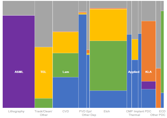
There is a wide variety of equipment needed in the semiconductor manufacturing process. Due to the advanced nature of these, each type is typically only manufactured by a limited number of players. Resulting in highly consolidated industries for practically all equipment types. Lithography, one of the key steps in the manufacturing process as here the chip’s patterns are laid out on the wafer, is dominated by ASML.
An illustration of the market shares for each type of equipment, from Applied Materials:
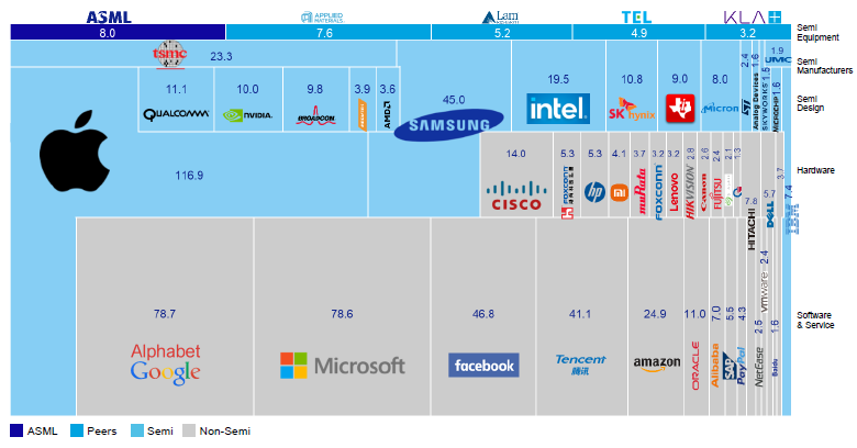
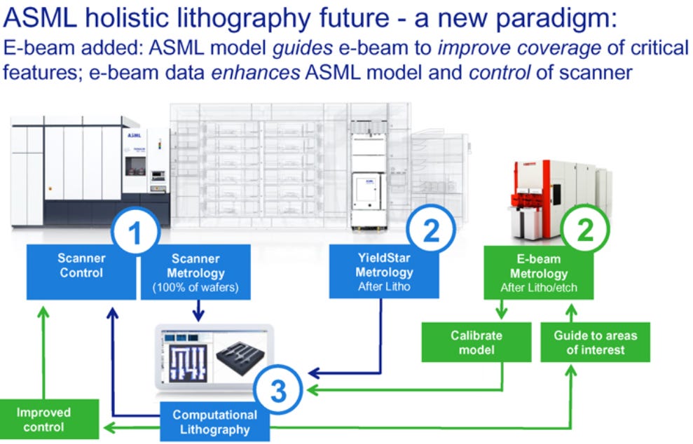
The below chart from ASML is a great visualization of the chip ecosystem. The tool manufacturers supply the fabs (TSMC, Samsung) who manufacture the chips developed by the designers (Nvidia, AMD). At the end of the supply chain are the customers such as Google and Microsoft.
Thoughts on ASML’s Q2 results and the semi cycle
ASML’s quarterly net bookings came in at EUR 4.5 billion, so Q1 might have turned out to be a cyclical low, although ASML’s CEO kept a cautious tone on the macro environment. This was echoed by TSMC’s management the next day. The bright spot in the macro picture was strong demand from more mature, lagging nodes in mainland China.
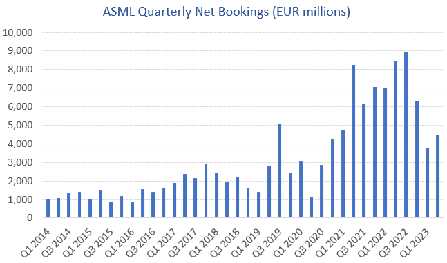
ASML’s equipment bookings clearly have been moving in a strongly upwards direction. This is driven by three factors:
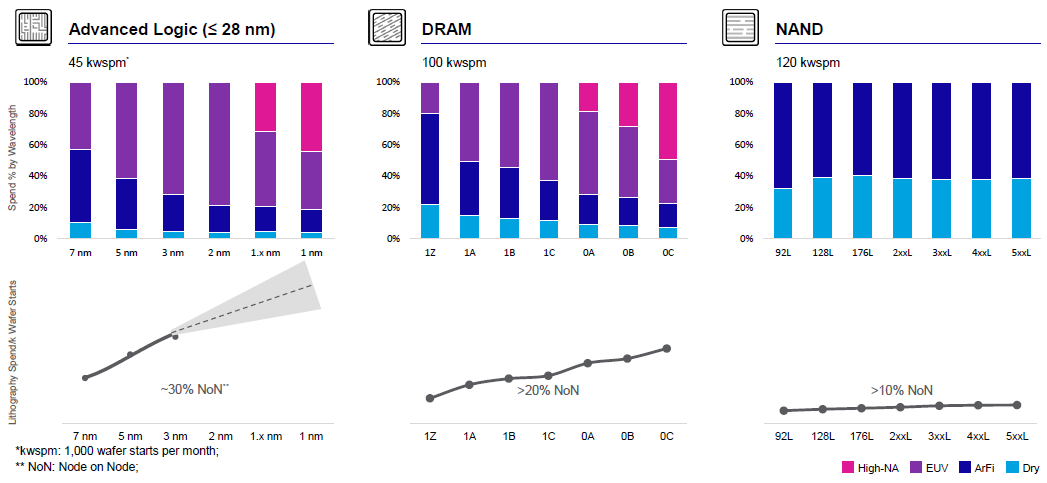
Firstly, capital intensity has been on the rise. For each new advanced semiconductor node, both more equipment as well as more advanced equipment are needed. Logic, i.e. computing processors, has been the really big driver of this, with litho spend rising around 30% node on node. In DRAM, working memory, we’ve seen a similar trend with litho intensity rising more than 20% node on node. NAND, i.e. storage memory, is much less litho intensive, as here memory cells are being stacked vertically as opposed to making transistors smaller as in Logic and DRAM.
ASML’s capital markets day illustrated these trends:
More advanced equipment means higher tool ASPs. EUV is currently the most advanced tool and on the Q2 conference call, ASML’s CFO noted that the next tool upgrade, i.e. the model 3800, will move pricing to above EUR 200 million. After that comes High-NA EUV, which has a better focus of the laser, allowing for an improvement in resolution of 40%. This basically means you’ll be able to build smaller transistors. Which has loads of benefits such as less power consumption and being able to cram more computing power in a single chip.
The chart below is somewhat old as EUV is already being priced at EUR 165 million, so not EUR 120 million like on the chart, but it illustrates well the trend of continuous price increases. This has been a big positive for ASML investors.

ASML’s CFO made the following interesting comments here:
The bookings for the 3800 are coming in because next year is going to show you a good blend of 3600 and 3800 tools. The 3800, we promised you that on this call, we would disclose the ASP, and the ASP is at least north of EUR 200 million. Even though it's a more expensive machine to make, bear in mind, there is quite some commonality in parts between the High-NA tool and the 3800 tool. So it will help both on the revenue side and also on the gross margin side, starting in '24. But definitely in '25 when the lion's share of the tools will be 3800s.
We're still on track for the first High-NA shipment in ‘24. We are seeing orders coming in, we're looking at double-digit numbers in the backlog and it's increasing. There is only a very limited number of customers for High-NA, and our customers really do not want us to disclose purchase order bookings. That's why we've not been sharing that data for quite a while now.
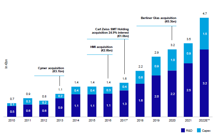
How an EUV tool looks like on the inside illustrated below. And ASML manufactures several of the key components themselves. The laser for example is manufactured by Cymer in the US, but they weren’t moving fast enough so ASML acquired them in 2013. They similarly took a stake in Carl Zeiss’ optical business to speed up production and R&D here as well. And more recently they also acquired Berliner Glass in the same optical arena. On top of that, ASML writes the software to improve the precision and productivity of the tools.
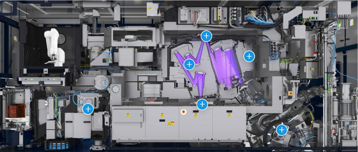
ASML similarly took over Taiwan based Hermes Microvision, a manufacturer of metrology tools. The main goal here was to enable a continuous feedback loop of metrology measurements into the EUV tool in order to recalibrate it during production.
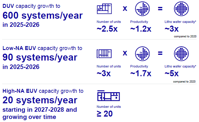
Looking at the production capacity of ASML’s tools, the company is lifting production in the medium term to 600 DUV tools per year, 90 EUV systems, and 20 High-NA ones. Last year’s capital markets day also highlighted how the productivity of the tools continuous to improve:
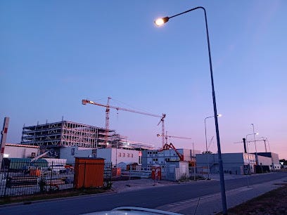
A photograph of construction works at ASML’s campus below, taken from Google Maps. Local press reports cite ‘a continuous emerging of new buildings, to the amazement of the local inhabitants’.
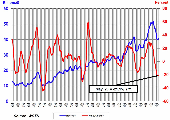
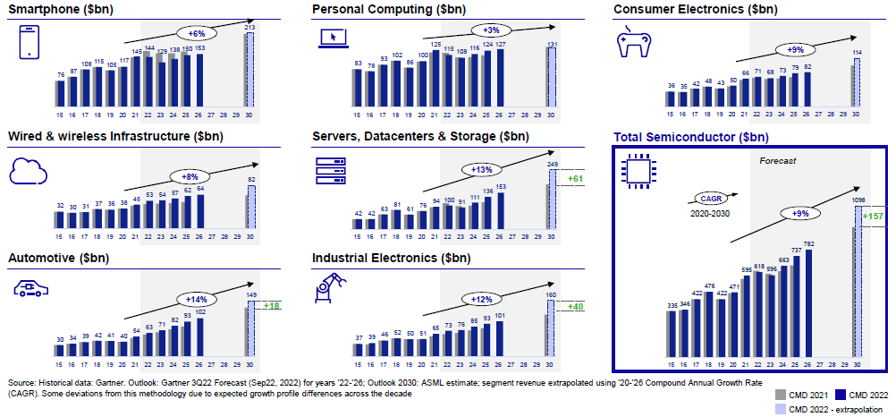
The second driver for ASML’s orders boom was driven by the covid semiconductor boom, resulting in widespread chip shortages and a strong demand for manufacturing equipment. SIA provides the following chart on global semiconductor revenues (the blue line):
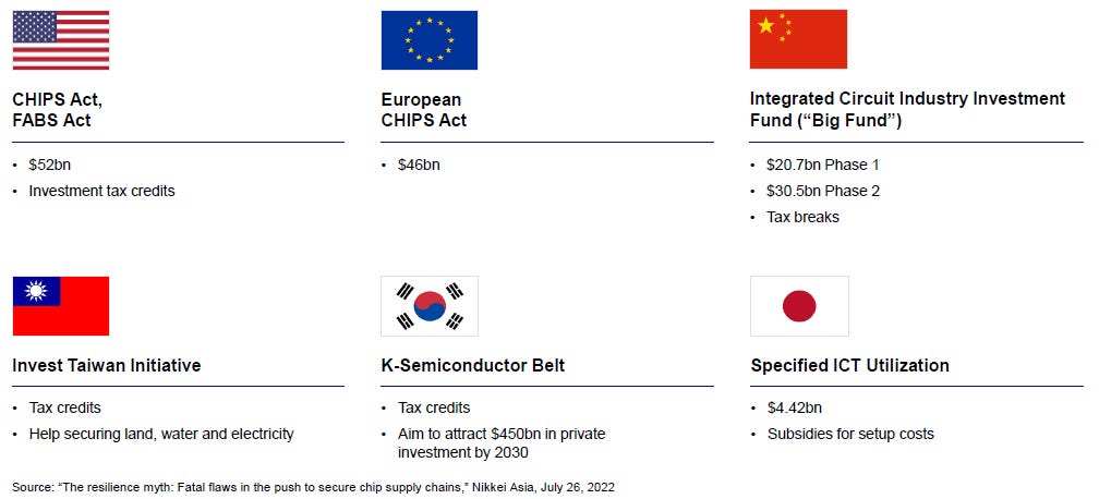
Third factor in ASML’s order boom, we’re also starting to see the effects of the new geopolitical cold war. Each geographic regional power is trying to secure its own semiconductor manufacturing capacity, from the US, to Europe, to Japan, and China.
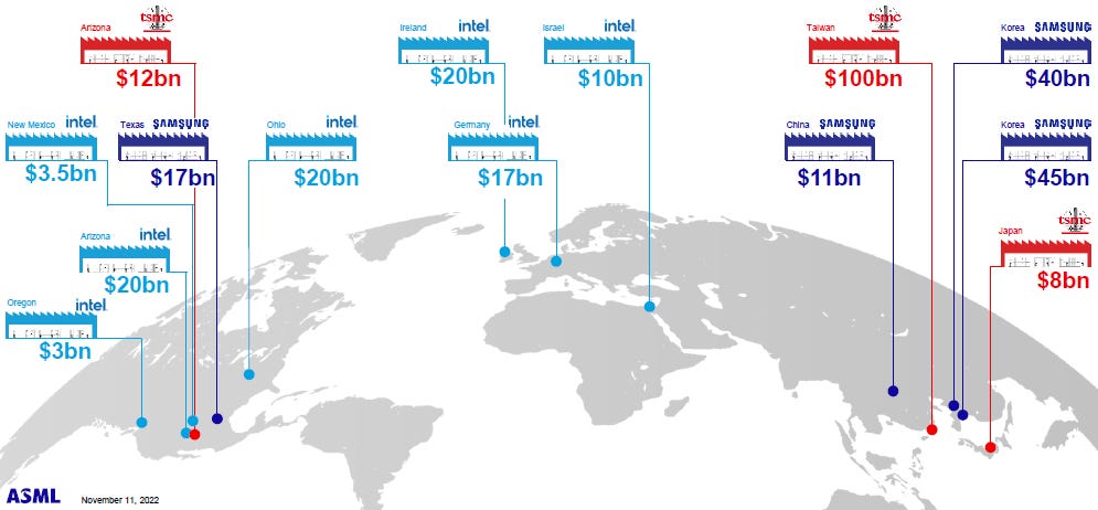
This is leading to a strong expansion of fabs around the world:
Strong Chinese demand from this strategic driver was actually a strong contributor in last quarter’s shipments. ASML’s CEO commented here as follows:
The concern of many of our Chinese customers is that given the increase of the geopolitical tensions, they do not want to rely on supply that comes out of China. So it's very simple that they're going to build a significant amount of capacity in that space, in the mid-critical to mature semiconductors to actually fuel those megatrends where China is actually leading. Think about the energy transition, the IoT in the industrial space, the rollout of the telecommunication infrastructure, battery technology, that's the sweet spot of mid-critical and mature semiconductors. And that's where China without any exception is leading. That's what's happening. Those fabs will be built. It's the strategic investment that drives the demand because it's the dependence that part of the Chinese industry has on imports.
Chinese locations took up 24% of ASML shipments in Q2 and is currently over 20% of the backlog.

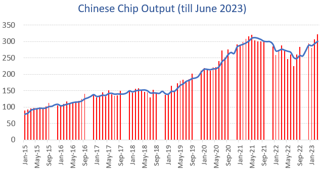
The Chinese Bureau of Statistics is confirming a high chip output from China-based semi manufacturers:
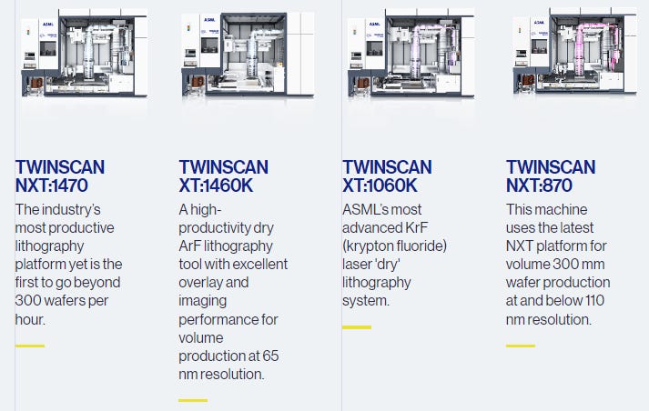
An overview of ASML’s DUV tools which the Chinese are currently buying loads of:
On the current macro environment and semi downturn, ASML’s CEO continued to have a more cautious tone:
Although certain end markets seem to be reaching the bottom of the cycle, the semiconductor industry is running at very high inventory levels, leading customers to moderate wafer output as the supply chain works to reduce and rebalance inventory levels. In order to limit wafer output, customers continue to run at lower litho tool utilization levels. Based on our view last quarter, customers were expecting a recovery in the second half of this year, but it now seems that this is more towards 2024. Customers remain cautious due to the uncertainty around the timing, the shape and the slope of the recovery.
In our EUV business, we have seen some shifts in demand timing. The majority of the shifts are due to fab readiness. We now expect to ship around 52 systems this year, translating to a year-over-year revenue growth for EUV of around 25% versus the previously communicated expectation of around 40%. DUV demand still exceeds supply. For the Installed Base business, customers are delaying productivity and performance upgrades on their litho systems. Therefore, we now expect our Installed Base business this year to be similar to last year versus a growth of around 5% as previously communicated.
I think in memory, it could be it's bottoming out, but we don't see a kind of an inflection point. The majority of the memory orderbook are basically technology transitions. They're just preparing for the next node transition, which needs EUV systems, the 3800s. In logic, it's very early but we could see some of an inflection point today. But that's just over the last short period. So see how sustainable that is.
Besides DRAM moving onto EUV, the next leg of growth will come from the leading edge logic players with the building out of their 2, 3, and 4 nanometer fabs. ASML’s CEO:
2025 clearly shows the opening and the first ramp of some significant advanced fabs in the logic space, for instance, the 2-nanometer fabs, 3-nanometer for all 3 leading customers. And that means we see significant opportunities also for growth in 2024. The order book looks good. We had an increase in bookings this quarter, resulting in a backlog of around EUR 38 billion exiting the second quarter. The firm demand looks good, but I'd love to see all of that being translated into orders over the next couple of quarters.
The semiconductor industry continuing to innovate is the strongest driver for ASML, as more tools and more advanced tools are needed in the manufacturing process. The technology roadmap looks as good as ever really. According to IMEC, the leading research house in transistor scaling, there’s an innovation pipeline till 2036 with continuous dimensional scaling. This means $ for ASML.
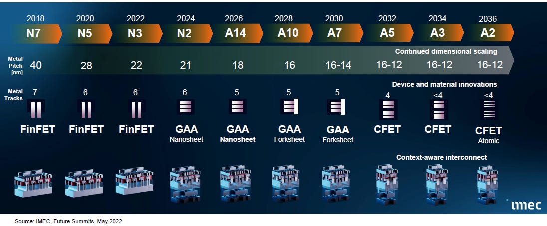
Also for DRAM and NAND there are clear technology roadmaps. ASML will benefit from this in DRAM, as here we have transistor scaling as well. But much less so in NAND, as this one is revolving currently around vertical cell stacking. Which happens to be more etch intensive. Tokyo Electron and Lam Research are examples of names which can benefit from this layering trend.
On the US-China chip wars, which have lead to export restrictions of advanced technology into China, ASML’s CEO gave the following update:
Due to these export control regulations, ASML will need to apply for export licenses with the Dutch government for all shipments of its most advanced immersion DUV lithography systems, which means the TWINSCAN NXT:2000i and subsequent immersion systems. We can ship our mid-critical immersion tools to China. As a reminder, sales of ASML's EUV tools have already been restricted.
There were also some reports in the media recently about additional US export controls. Of course, we will and cannot respond to speculation. However, based on our current understanding, we do not expect to change our previously communicated view. Therefore, based on everything we have been made aware of as of today, we do not expect the Dutch and potential additional US measures to have a material impact on our financial outlook for 2023 nor on our longer-term scenarios as communicated during our investor day in November last year.
And my hunch about what the Dutch were finally going to say in the end was about right. And I also have a kind of a hunch on what's going to happen for the rest of the year and with the new rules. And my gut feel is based on what we hear and our understanding, it’s not going to have a material impact. But we just have to wait. I think Japan came out, the Dutch came out. I think the US government will probably come out soon. And then we'll know for sure whether my hunch or my gut feel is correct.
Financials - share price at time of analysis is EUR 620 on the Amsterdam Stock Exchange
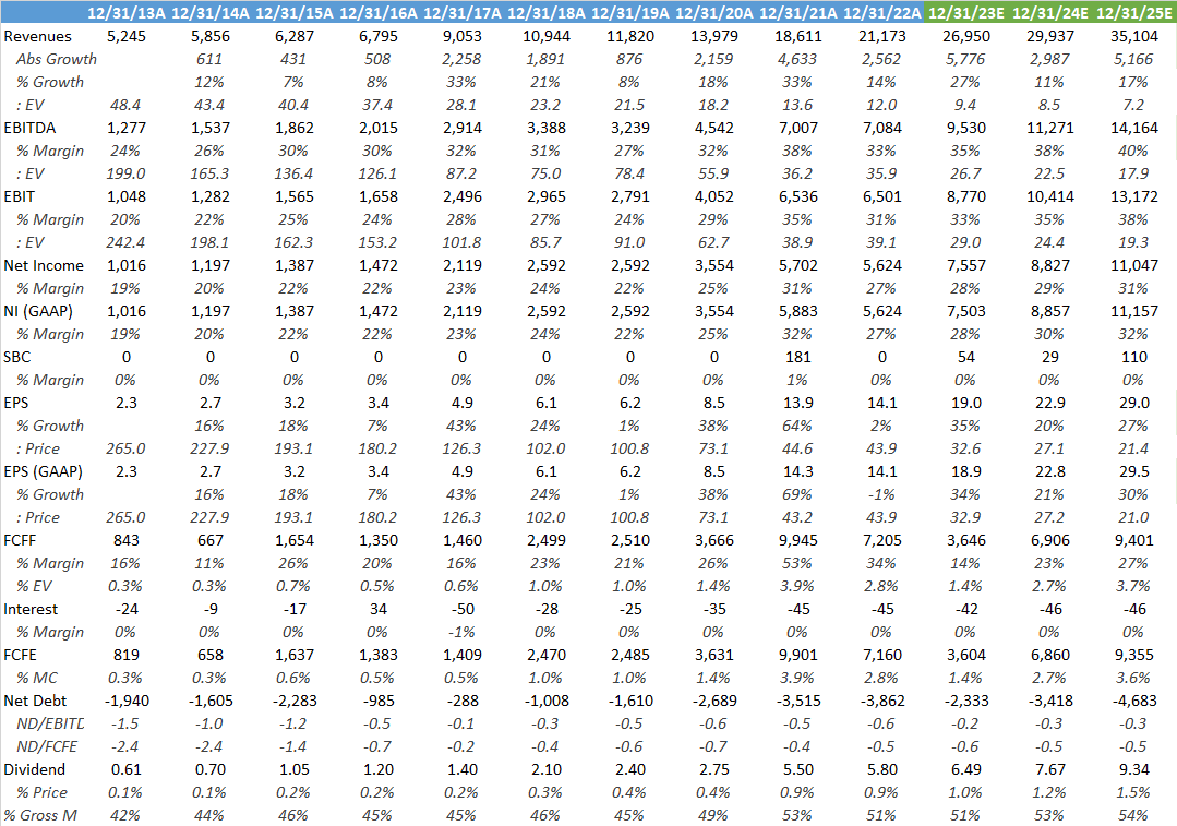
Currently analysts are modelling in strong growth rates for ASML to continue and with a EUR 38 billion backlog, the numbers for the coming eighteen months are basically in the bag. Then as the orders start filling up as TSMC, Samsung, and Intel will be looking to battle it out at 2-3-4 nanometers, this will provide the next leg of growth.
The above revenue growth has been driven by ASML’s R&D prowess, which they are continuing to step up:
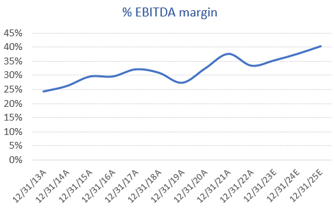
Despite these increasing investments, ASML has had a solidly improving EBITDA margin profile. On top of that, I do believe they are underpricing their tools, more on this later.
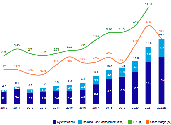
Around 25% of the business is now starting to come from Installed Base Management, which are services and spare parts to improve the productivity of ASML’s tools in the field. This is a highly attractive business for investors as it is much less cyclical than order flow.
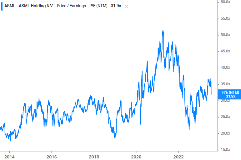
Analysts are forecasting double-digit top line growth to continue. If ASML can hit those 2025 consensus numbers, the shares would be valued at an attractive 21x EPS. Taking into account the dividend yield and share buybacks, I get to a 31% IRR putting those 2025 numbers on a 30x next-twelve-months’ PE.
As more investors have grown aware of the ASML story, it’s multiple has moved upward over time. However, as long as ASML’s fundamentals remain intact, i.e. the monopolist lithography provider exposed to double-digit top line growth rates, I do believe that this multiple of around 30x PE NTM could hold for quite a while.
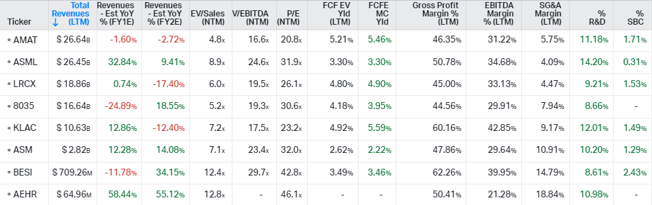
Compared to peers, ASML has the highest R&D intensity, at 14% of sales and has one of the best near term growth profiles based on analyst estimates. There is also clear upside on the gross margins, one could argue that ASML is probably underpricing their tools to help the semiconductor industry. As their tools are incredibly expensive, underpricing these helps somewhat with the build-out of fabs around the world and especially with the transitioning to next-gen technologies.
Long term model
During the Q2 call, ASML’s CFO confirmed the company’s gross margin target of around 55% for 2025, which the company set at their latest capital markets day. The main driver will be the production of the EUV 3800 model having ramped up. Longer term, the company guides gross margins to continue to move north as also the High-NA tool goes into production.
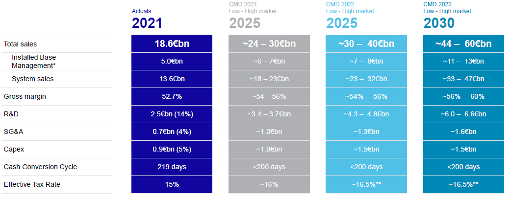
At their latest capital markets day, ASML updated their long term model for 2030. Even if ASML would hit the low end of their guidance and the shares de-rate to a 25x PE, investors could still make a double digit internal rate of return (IRR). The easiest way to think about an IRR is to see it as annualized return. This number can be easily compared to your cost of risk, which is typically around 8% or so. IRRs well above the cost of risk are typically seen as wise investments.
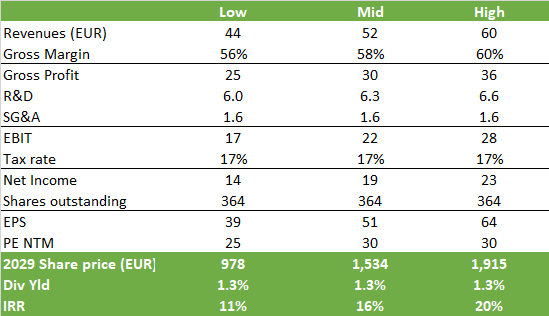
In the above calculation, I’m also factoring in ASML continuing to buy back shares at a rate of 1% of outstanding shares per annum, which reduces the share count by 2030 and lifts EPS. But this number could easily be higher, as ASML has been buying back 2-3% of its shares over the last few years.
Below is the detail on how many tools of each type ASML is assuming to ship under both the high and low scenarios:
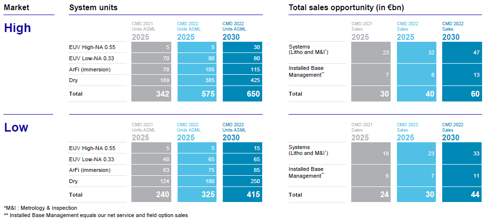
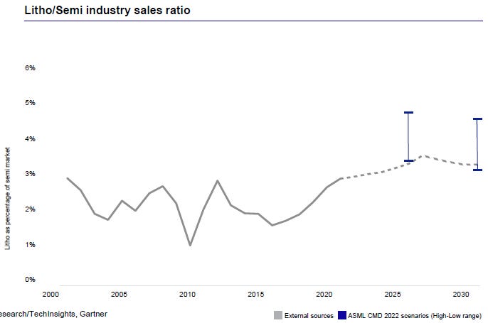
For this long term model, ASML is assuming the industry’s litho spend relative to semiconductor sales to increase from 2-3% to 3-4.5%. In my view, this looks fairly manageable for the industry, taking into account that ASML is the key enabler of transistor scaling.
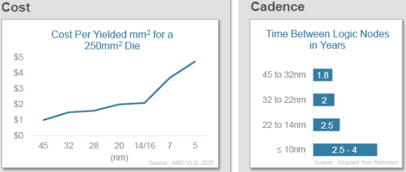
The main risk for ASML is the semiconductor innovation roadmap continuing to slow down, which would result in order flow per node getting spread out over more years, lowering annual revenues. The other risk is on the economics, with the cost per die area having taken on a much steeper slope post 16nm. However, my view is that additional costs can be partly recuperated from lower energy bills due to the efficiency gains of smaller transistor sizes. Additionally, these next-gen transistors bring other benefits, such as faster computations, more calculation power, and longer battery lifes. I suspect most of the leading edge customers, e.g. Nvidia, Apple and AMD, will continue to be happy to pay for this, also as they need to differentiate their products anyways.
The other point to note here is that ASML doesn’t grasp these numbers out of thin air, there are regular discussions along the supply chain with the managements of TSMC, Intel and Samsung about how much capacity those are planning to install at 4, 3 and 2nm and how much immersion, EUV and High-NA tools they need for this. These fabs need ASML to be ready so it’s in their own interest to communicate clearly on their capacity needs. There are extreme amounts of collaboration across the leading edge semi supply chain to push innovation forward. This gives ASML an extremely good view on the market potential for their tools.
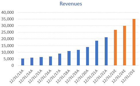
Ten years ago, ASML came out with their EUR 10 billion 2020 revenues target. Many laughed at the time but ASML flew right past that and is going to do EUR 27 billion of revenues this year. The graveyard of ASML bears is long and a wide one.
Conclusion
ASML’s shares were weak post results, down 8% over the last five trading days at the moment of writing, as obviously the near term outlook was revised downwards somewhat and then the day after TSMC came out with a weak Q2 while lowering their capex forecast for the year. Should economists be correct that we’re heading into a recession, this would obviously send the shares further south in the coming year. However, taking a long term view, the prospects for ASML still look tremendously bright. In my opinion, cyclical pullbacks in the share price are likely to provide nice entry points for long term investors.
Where else to position in semiconductors besides semicap? Semi companies exposed to the datacenter, automotive, and industrial end-markets are expected to see the highest growth rates. Some of the names I like here currently include Valens Semi and Alphawave Semi, but I’ll be reviewing more companies in these spaces so make sure to hit subscribe.
If you enjoy research like this, hit the like button and share a link on social media or with colleagues with a positive comment, it will help the publication to grow.
I’m also regularly discussing technology investments on my Twitter.
Disclaimer - This article is not advice to buy or sell the mentioned securities, it is purely for informational purposes. While I’ve aimed to use accurate and reliable information in writing this, it cannot be guaranteed that all information used is of such nature. The views expressed in this article may change over time without giving notice. The mentioned securities’ future performances remain uncertain, with both upside as well as downside scenarios possible.
Great write up as usual. Reading between the lines of TSMC recent Arizona fab delay announcement, it seems like there simply is not enough American engineers competent/knowledgeable enough operate the machines like EUV etc that will be going into these new Chips Act-induced North American fabs. I’m wondering if there’s provisions in the Act to promote and turbo-charge U.S semiconductor engineering education, because we need more of them.